
Lab in charge:
- Faculty: Prof. Riyaz R
- Technical Staff: Mr. Satheesh Kumar S
Details of Labs conducted:
- ECL203 – LOGIC DESIGN LAB – S3 AEI, S3 ECE
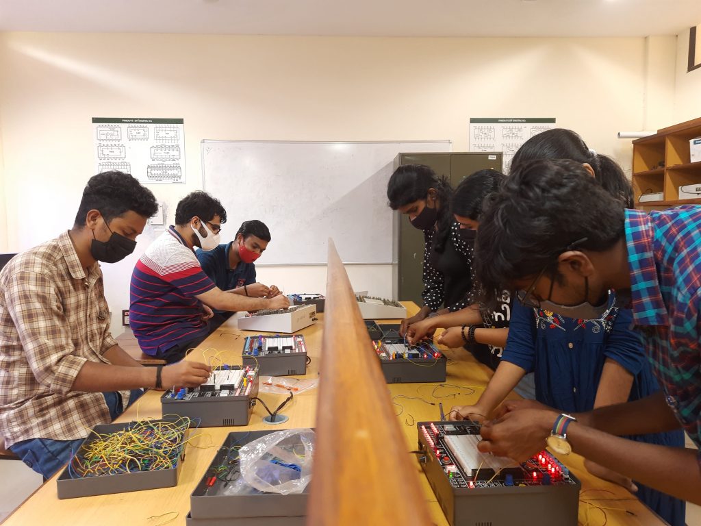
ECL203 – LOGIC DESIGN LAB
This course aims to:
- Familiarize students with the Digital Logic Design through the implementation of Logic Circuits using ICs of basic logic gates
- Familiarize students with the HDL based Digital Design Flow.
LIST OF EXPERIMENTS:
Part A
The following experiements can be conducted on breadboard or trainer kits.
1. Realization of functions using basic and universal gates (SOP and POS forms).
2. Design and Realization of half /full adder and subtractor using basic gates and universal gates.
3. 4 bit adder/subtractor and BCD adder using 7483.
4. Study of Flip Flops: S-R, D, T, JK and Master Slave JK FF using NAND gates
5. Asynchronous Counter:3 bit up/down counter
6. Asynchronous Counter:Realization of Mod N counter
7. Synchronous Counter: Realization of 4-bit up/down counter.
8. Synchronous Counter: Realization of Mod-N counters.
9. Ring counter and Johnson Counter. (using FF & 7495).
10. Realization of counters using IC’s (7490, 7492, 7493)
11. Multiplexers and De-multiplexers using gates and ICs. (74150, 74154)
12. Realization of combinational circuits using MUX & DEMUX.
13. Random Sequence generator using LFSR.
Part B
1. Realization of Logic Gates and Familiarization of FPGAs
2. Adders in Verilog
3. Mux and Demux in Verilog
4. Flipflops and coutners
5. . Multiplexer and Logic Implementation in FPGA
6. Flip-Flops and their Conversion in FPGA
7. Asynchronous and Synchronous Counters in FPGA
8. Universal Shift Register in FPGA
9. BCD to Seven Segment Decoder in FPGA